|
|
 |
 |

|
| |
RECYCLABLE
HOLOGRAPHIC STORAGE MEDIA
Joseph
Bordogna, Scott A.Keneman,
Juan
J. Amodei
Moore
School of Electrical Engineering,University of
Pennsylvania,
Philadelphia,USA
RCA
Laboratories, Princeton, New Jersey, USA
Itek
Corporation, Lexington, Massachusetts, USA
Performance
parameters of state-of-the-art recyclable holographic recording
madia are compared to develope tradeoffs for their use in
holographic storage and imaging applications. Included are
record energy, recoed time, erase time, diffraction efficiency,
linearity, resolution, cycle lifetime, natural decay time,
and a figure of merit. Materials and devices discussed include:
magneto-optic, electroptic, and photochromic materials;
metal films; ferroelectric-photoconductor, thermoplastic
deformation, elastomer, liquid crystal-photoconductor-Pookel's
effect devices.
INTRODUCTION
The
advent of the laser as a reliable commercial product has
made possible the use of optical holography for information
storage, processing, display, and image conversion system
/1-3/. It is the purpose of this paper to discuss briefly
and compare the materials /4/ and devices which researchers
hope will store the holographic data and perform the real-time
holographic imaging in such systems. In particular, an overview
is given of the physical basis, fabrication, and operating
parameters of available holographic storage media.
Recyclable
media are characterised by their ability to be era-
sed
and reused for sequentially storing different information
patterns. Referring to such media as "holographic" implies,
at least, that they are capable of supporting micrometer
resolution. "Storage" implies an ability of the medium to
keep the information interact after the hologram is recorded.
In view of the embryonic state of development of light sensitive
media for information applications this paper is not limited
in scope only to media that satisfy the above criteria;
materials and devices which satisfy some, but not all, of
the requirements of ideal recyclable holographic storage
media are discussed. Some media possess insufficient resolution;
others are subject to decay. Some make no attempt at permanence
but are useful for holographic imaging. Others fatigue after
numerous operating cycles. We include materials subject
to these deficiencies because it is likely that as technology
advances and the understanding of the various media increases,
some of these deficiencies may be removed and the realization
of higher performance recyclable holographic storage media
achieved.
The
media discussed may be characterized as materials
or devicies depending on their fabrication and use. The
former possess a single constituent which is directly light
sensitive. The latter are composite structures containing
a light sensitive element but requiring more than light
along to operate properly. The materials discussed
include magneto-optic films, electro-optic crystals, photochromatic
materials, and metal films. The devices include feroelectric-photoconductor
devices, thermoplastic deformation devices, elastomer devices*,
photoconductor-liquid crystal devices, and photoconductor-Pockel.'s
effect devices.
The
media are compared on a number of operating parameters:
record or write energy (quantity of energy per unit area
required for recording-frequently referred to as "sensitivity");
re-
cord
time (time required to record a hologram); erase time (time
to clear storage medium for next hologram); diffraction
efficiency (percentage of light energy in reconstructed
image to incident energy of readout light); linearity (measure
of attainable contrast or "gray scale"); resolution capability
(number of resolvable lines per linear distance); cycle
lifetime(number of times medium can be recorded and erased
without deterioration of performance); and natural decay
time (length of time hologram can be stored with no sustaining
power). A comparison summary is presented in Table 1. Unfortunately,
this table does not tell the complete story. Factors such
as difficulty of fabrication, reproducibllity of parameters,
and projected eventual cost are missing. Further research
on these and other factors is in progress.
MAGNETO-OPTIC
REGORDIMQ MATERIALS
Curie
point writing on manganese-bismuth films /5-10/ can be used
for direct storage of digital information or for holographic
storage or digital or pictorial information. Writting is
achieved by switching the magnetieation of a semitransparent
film (~ 300 to 700 nm thick) in response to the heating
caused by local light absorption. Readout can be accomplished
through the magneto-optic Faraday or Kerr effect which gives
rise to rotation of the polarisation of the light transmitted
or reflected. Because the writing mechanism relies on selectively
heating the film above the Curie temperature in the region
of higher light intensity, while leaving the regions of
low intensity below the Curie temperature, this medium requires
that writing be accomplished in times that are short compared
to the thermal time constant of the film this time is normally
of the order of 100 nanoseconds. This calls for high power
pulses lasers, or focused CW lasers for high resolution
writing, in order to supply the energy necessary to reach
the Curie teaperatare in a sufficiently short
Table
1. Performance Parameters for Recyclable Holographic Storage
Media.
|
Storage
medium
|
Material
or principal material in device
|
Reference
|
Recording
and Erasure
|
|
Recording
Process
|
Write
Energy (mJ*cm-2)
|
Record
Time
|
Erase
Process
|
Erase
Time
|
|
Magneto-Optic
Materials
|
MnBi
|
5-13
|
Heating
above Curie point
|
10
|
10ps
50ns
|
Same
as recording
|
~μs
|
|
Electro-Optic
Materials
|
LiNbO3
|
14-19
|
Optically
induced charge separation
|
103-5*105
|
10s-min
|
Optically
or thermally induced charge re-distribution
|
Same
as record
|
|
Photo-Chromic
Materials
|
Many
Types (see text)
|
20-29
|
Optically
induced charge transfer
|
50
|
~ns
|
Same
as recording
|
Same
as record
|
|
Metal
Films
|
Bi
|
30
|
Evaporation
by heating
|
50
|
5-20ns
|
Redistribution
by contained evaporation
|
~1s
|
|
Ferro-electronic
Photo-conduction Devices
|
Bi4Ti3O12
PLZT
|
38-43
34,
35
|
Light
modulated ferroelectric switching
|
1
10
|
~ms
~s
|
Same
as recording
|
Same
as record
Same
or less than record
|
|
Thermo-plastic
Deforma-tion Devi-ces
|
Stay-
belite
|
47-55
|
Electr.
Field produced deformation of heated material
|
10-3
(theo-retical)
|
1
ms
|
Heat
|
~1s
|
|
Elastomer
Devices
|
Siloxane
(-ru- ticon)
|
56
|
Electric
field produced deformation
|
10-1
|
~ms
|
Removal
of electric field
|
~10ms
|
|
Liquid
Crystal Photo-conductor Devices
|
Mixed
liquid crystal; ZnS, CdS, photo conductor
|
59-60
|
Light
modulated dynamic scattering
|
~5*10-3
|
<0.1
ms
|
Appication
of ac electric field
|
20-500
ms
|
|
Photo-conductor
Pockel's Efeect Devices
|
Bi12SiO2
|
61-63
|
Light
modulated electro-opt effect
|
~10-4
|
~μs
|
Light
at appropriate wavelenth
|
~μs
|
|
Readout
|
Cycle
Lifetime
|
Decay
Time (Dark Storage)
|
Figure
of Merit
|
|
Type
of Hologram
|
Readout
efficiency (%)
|
Linearity
|
Resolution
(lp*mm-1)
|
Write-Erasure
|
Read
|
|
Thin
phase
|
10-2
(Fara-day)
10-1
(Kerr)
|
Fair
|
~1000
|
Indefinite
|
|
Indefinite-limited
by humidity
|
100
|
|
Thick
phase
|
80
|
Good
|
~1500
|
Indefinite
|
Reading
at same as writing destroys information
|
Weeks
to months
|
24
|
|
Amplitude
|
1,2
3,7
|
Very
good
|
~10,000
|
Indefinite
|
Blea-ching
occurs
|
Minutes
to months
|
740
|
|
Amplitude
|
6
|
Good
|
~1000
|
~10
cycles
|
|
Indefinite
|
120
|
|
Thin
phase
|
10-2
Unknown
|
Fair
Good
|
~800
~50
|
~105
cycles
Limited
by fatique (see text)
|
Indefinite
|
Indefinite
|
Readout
efficiency unknown
|
|
Thin
phase
|
15
|
Good
|
~1000
|
100
cycles
|
|
Indefinite
|
7*106
(theo-retical)
|
|
Thin
phase
|
15
|
Good
|
~1000
|
>104
cycles
|
Depends
on device structure
|
Not
a permanent storage device
|
1,5*105
|
|
Thin
phase
|
Unknown
|
Good
|
~10
|
Unknown
|
Unknown
|
Unknown
|
Readout
efficiency unknown
|
|
Thin
phase
|
Unknown
|
Good
|
~1000
|
Unknown
|
Unknown
|
~hours
|
Readout
efficiency unknown
|
time.
Erasure of the pattern is accomplished by uniformly remagnetizing
the film by means of an external magnetic field. The film
deposition technique and other details of the operation
and recording process are discussed at length by Mezrich
and Cohen elewhere in this issue*.
The
most common magneto-optic recording material is manganese
bismuth (MnBi). Its pertinent performance parameters are
listed in Table 1. Other important parameters include: Faraday
rotation > 5*105 degrees/cm-1,
Kerr rotation ≈3°; absorption coefficient =3,5*105
cm-1; additional physical parameters are given
by Mezrich and Cohen*. Perhaps one of the most
serious disad vantagee of MnBi is its performance deterioration
under humidity conditions greater than 50%; however, this
effect is not completely understood as yet /11/.
Other
materials being investigated include gadolinium-iron-garnet
(GdIG) /12/* and europium oxide (EuO)/13/*,
EuO has a major disadvantage in that it operates only at
liquid helium temperatures. All things considered, MnBi
appears to be the best candidate for magneto-optic holographic
storage at the present state of the art.
ELECTRO-OPTIC
RECORDING MATERIALS
High
efficiency volume phase holograms can be recorded in certain
transparent electro-optic crystals. Examples are lithium
niobate co-doped with iron (LiBbO3 : < Fe),
lithium tantalate (LiTaO3), strontium-barium
niobate [(Sr,Ba)Nb2O6, SBN, or Ba0.75Sr0.25Nb2O6],
and doped barium - sodium niobate
(Ba2NaNb5O15)/14-18/.
The
recording process relies on the optical excitation and subsequent
frift or diffusion of electrons which originate from localized
centers in the crystal. This creates fields that modulate
the index of refraction of the material and the result in
a phase hologram whose efficiency could theoretically be
as high as 100%. Proper recording procedure requires that
the crystal optic axis be perpendicular to the fringe gratings
of the hologram. High efficiency readout can be accomplished
only with light polarized in the plane containing the optic
axis.
Holographic
diffraction efficiencies as high as 80% have been achieved
in LiNbO3 : Fe crystals which are about 0,2 cm
thick. The sensitivity of this material (which is relatively
low compared to other recording materials) varies between
1 and 500 J*cm-2 (at λ=488nm) depending
on the doping or other treatment to which the material was
subjected. Storage times of many days are possible at ordinary
room illumination levels and erasure can be achieved either
optically or by beating the crystal to 300°C. The holograms
stored in the material can be "fixed" utilising a simple
thermal process which causes the patterns to be optically
nonerasable /19/. Application of an electric field has been
shown to improve the performance of (Ba,Sr)Nb2O6
as an electro-optic recording material /15/ but the published
diffraction efficiencies (2%) are considerably lower than
in LiNbO3 and LiTaO3. Details on LiNbO3
and doped LiNbO3 are given elsewhere in this
issue*.
In addition
to the materials discussed above, several other electro-optic
hosts have been tried but with only marginal success. These
include barium titanate (BaTiO3), bismuth oxide
(Bi12SiO20), and bismuth germanate
(Bi4Ge3O12)/17,18/.
PHOTOCHROMIC
MATERIALS
Color
centers in transparent crystals are caused by the presence
of impurities and imperfections which give rise to localized
states that trap electrons or holes within the forbidden
energy gap of the material /21/. Such states may show absorption
at visible wavelengths where the pure crystal is transparent.
In particular, the photochromies materials have the ability
to switch colors under the influence of optical irradiation.
This change is normally caused by the transfer of an optically
excited electron from one type of color center to another
with the absorption properties of both centers being changed
accordingly. Light of one wavelength produces a given change
in coloration, and the crystal returns to its original state
when exposed to light of another wavelength.
The
performance of inorganic photochromies can be compared to
other media by referring to Table 1. They are characterited
by the maximum absorption change induced by light, the energy
required to produce a given change, the background absorption,
and the storage time of the material. The inherent resolution
of the materials is practically unlimited as illustrated
by the fact that reflection holograms with fringe spacing
of less than 100 nm have been successfully recorded by Amodei
in SrTiO3 : Pe, Mo.
The
sensitivity of inorganic photochromic materials varies considerably
from hundreds of J*cm-2 to nJ*cm-2
depending on the quantum efficiency of the process. The
maximum storage time of the crystals, which is usually determined
by the thermal activation energy of the centers, varies
from minutes to months.
Examples
of inorganic photochromic materials include silver
halide photochromic glasses /20-23/, and inorganic photochromio
crystals (e.g. SrTiO3:Fe, Mo; BaF2:La;
Sodalite:Cl, electron beam colored NaCl; and fluorescein-boric
acid glar organophosphor) /24-26/.
Successful
cyclic recording and erasure of holographic infor-
nation
on thin organic photochromic films has been reported
by Milcaeliane and hia assooiates in the Soviet Union /28/,
and N.Lescinsky and M.Miller in Czechoslovakia /28/. Performance
data for these materials(essentially photochromic epiropyran
dissolved in styrene polymer) are rather sketchy at this
time, however. In the United States, Ross /29/ has investigated
the use of thioindige dye. The efficiency of the material
is temperature dependent, but its densities are higher than
those of the inorganic photochroioic materials.
In summary,
a clearly destinot advantage of photochromic materials is
that there is no inherent resolution limit since absorption
takes place on an atomic or molecular scale. Disadvantages
include: sensitivity limited to narrow spectral regions;
relatively thick samples (1-10 mm) required to obtain useful
optical densities; and image deterioration due to both thermal
decay and optical bleaching during readout.
METAL
FILMS
Concentrated
layer energy may be used to raise the temperature of a material
to its vaporization point. This principle has been used
to store evaporation holograms in thin metal films /30/.
Films may initially be deposited on substrates using conventional
technology. Then, during hologram recording, locations of
constructive interference rise to higher temperatures than
do points of destructive interference.
Holographic
recording by vaporation relies on the fact that the energy
absorbed by a thin film (7,5 - 20 nm) during a very short
laser pulse does not have time to diffuse away. Exposure
to such light pulses, therefore, causes the material to
vaporise from each point of the surface in amounts that
are nearly proportional to the integrated intensity of the
light absorbed at that point. When a holographic intensity
pattern is applied to a film in this manner, it leaves a
film thickness profile which closely resembles the spatial
intensity variations of the recording light. Such a pattern
is considered an amplitude ho-
logram
because, while the absorption is substantial, the film is
not sufficiently thick to significantly affect the phase
of the light traversing it. The hologram thus stored can
be read out by reflection or transmission with comparable
efficiencies. In tests with 7,5-20 nm thick bismuth (Bi)
films vacuum deposited on glass substrates /30/, both transmission
and reflection holograms have efficiencies of 6%, which
is very close to the theoretical maximum for amplitude holograms.
The
sensitivity of this direct holographic recording material
depends to some extent on film thickness; for films approximately
10 nm thick, the energy required to record was experimentally
/30/ found to be less than 50 mJ/cm2, which compares
favorably with other materials such as photochromies and
magneto-optic thin films (see Table 1).
Another
feature of the thin metal films is that they may be operated
in a linear region because the energy required to reach
boiling temperature is much lower than the vaporation energy.
Also, since the recording technique is heat rather than
light dependent, lasers of any wavelength can be used for
recording. A chief disadvantage, of course, is the difficulty
in recycling. It is possible to build a contained cell where
the material is evaporated between two surfaces in very
close proximity and is thus redistributed during the recording
cycle. Such a device could then, in principle, be erased
by exposure to a spatially uniform light pulse that redistributes
the film evenly over the surface. Experiments by Amodei
have shown that this approach is feasible, at least for
a limited number of cycles (5 to 10), and it is conceivable
that with proper de -sign, cycle lifetime could be extended
considerably.
FERROELECTRIC-PHOTOCONDUCTOR
DEVICES
The
use of a ferroelectric-photoconductor sandwich device for
information storage is not a particularly new idea /31/.
However, it is only recently that the suggestion was made
to operate such a device with optical readout /32/. Early
devices in-
corporated
an optically controlled record operation but readout was
electrical.
In many
ferroelectric materials the two stable remanent polarisation
(PR) states may not be distinguished optically.
Recently, two material configurations not posseasing this
disadvantage have been suggested: (1) use of ferroelactric
bithmuth titanate, Bi4Ti3O12,
in which non-180° switching of PR may be performed
/33/, and (2) "strain-biasing" of ceramic PLZT ferroelectrics
to allow effectively non-180° switching of PR
/34,35/. With these ferroelectric materials, ferroelectric-photoconductor
(PE-PC) devices capable of optical (with applied electric
field) record and optical readout are possible.
The
PE-PC device geometry ia shown schematically in Fig.la.
The ferroelectric (FB) slab (either single crystal, ceramic,
or thin film) is covered with a photoconductive (PC) layer,
and the combination is sandwiched between transparent electrodes.
External batteries or pulse generators are used to apply
switching fields to the device. The operational characteristics
of the PB-PC device are determined by the specific materials
used. Two typical state-of-the art materials are Bi4Ti3O12
and strain-biased PLZT.
Bismuth
titanate, a member of crystal class m /33/, is prepared
in single crystal platelets by flux growth /36/. It posseses
four atable remanent polarisation states (having both a-axis
and a-axis components) in a detwinned cryetal. By first
poling /37/ PRa (in the plane of the crystal)
uniformly, switching PRc between its two states
leads to the non-180° switching described earlier. As shown
in Fig.1b the orientations of the optical indicatrix for
the two states differ by a rotation of 2a (roughly 50°)
around the crystalline b(x3)-axis. Since Bi4Ti3O12
is biaxial, n11≠n22≠n33.
Two teehniques for observing for cohange in optical indicatix
orientation (or equivalently, reading out a stored pattern
in an FE-PC device) are possible: (1) tilting the crystal
about the a-axis to achieve a difference in extinction directions
for the two states /32, 38, 39,40/ (illustrated In Fig.la),
and (2) tilting the crystal about the c-
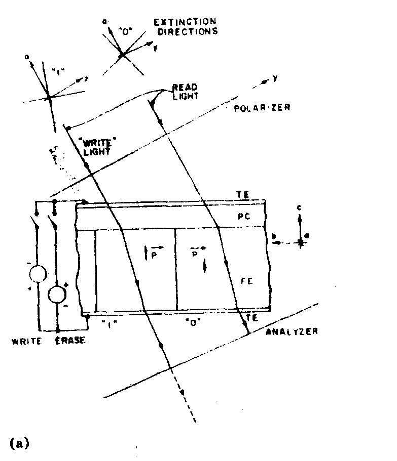
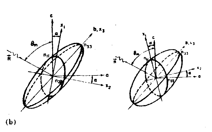
Fig.1.FE-PC
(a) Bi4Ti3O12 device geometry
showing WRITE and READ processes and (b) orientation of
optical indicatrix for Bi4Ti3O12
for the two states of c-axis remanent polarisation PRc
(with fixed PRa).
axis
to achieve a phase difference for light polarized perpendicular
to b /39,41/. The reader may easily convince himself that
light normal to the ab plane (i.e., parallel to the c -axis)
will not be adequate to distinguish the two dates. Both
techniques have been used to reconstruct holograms stored
in FE-PC devices /38-41/.
PL2T
(lanthanum-doped lead zirconate-lead titanate ceramic material)
platelets /34/ coated with photoconductor layer and transparent
electrodes, are held intension or compression causing ferroelectric
domains to line up parallel and antiparallel to the strain
axis (in the platelet) resulting in zero net remanent polarization.
By switching the device with fields normal to the platelet
a normal component of remanent polarization, allowing readout
of a stored pattern.
Both
bismuth titanate and PLZT FE-PC devices are included among
the comparisons in Table 1. To date, holographic storage
has only been reported in the former. Both devices possess
their own unique advantages and disadvantages. Both possess
an inherent gain mechanism, similar to that in photographic
film. Incident light for recording does not directly cause
the storage; rather, photoeleotrons in the photoconductor
are "created" by the light causing an increase in conductivity
and allowing the battery to switch the ferroelectric. The
bismuth titanate device involves difficult fabrication and
processing techniques because of its single-crystal nature,
large-area devices are difficult to achieve. Furthermore,
an optical degradation has been observed after numerous
switching cycles with metal electrodes directly on the Bi4Ti3O12
surfaces /42/. However, such degradation has not yet been
observed in FE-PC devices with photoconductive layers /43/.
The
PLZT device is simpler to fabricate because of its ceramic
form. However, ferroelectric ceramics are notorious for
their electrical and optical fatigue /44/, which would restrict
their useful lifetime.
Perhaps
the ultimate FE-PC for holographic applications would utilize
thin films of Bi4Ti3O12.
Such films have recently
bean
produced /45,46/. They might represent the optimum compromise
between the diffioulties of single-crystal technologies
and long term ceramic fatigue.
THERMOPLASTIC
DEFORMATION DEVICES
The
technique of thermoplastic recording was first described
by Glenn in 1959 /47,48/. Prior to its application to holography,
this recording technique used an electron beam to scan a
thermoplastic film (e.g., polystyrene, chlorinated polyphenyl,
or alphamethylstyrene) and record video signals in the form
of a pictorial image; the image was visible on the film
immediately following recording. The technique offered very
high resolution and recording bandwidth with the option
of erasure if desired.
The
making of phase holograms on thermoplastic film was first
demonstrated by Urbach and Meier in 1966 /49/. As most recently
described /50/, a phase hologram is recorded in a transparent
thermoplastic film as a spatial variation of film thicknens
corresponding to the light intansity variation of a holographic
fringe pattern. Since the thermoplastic is usually a light-intensive
resin, it is combined with a photoconduotor in a film structure
which can respond to light. Although manufactoring a film
structure with the photoconductor dispersed through the
thermoplastic is possible, the usual structure consists
of a layar of thermoplastic coated over a layer of photoconductor
bacause it yields higher photosensitivity /50/. The complete
structure consists of a glass substrate covered by a grounded
transparent conductive film on top of which lie the photoconductor
and thermoplastic film. The sequence of a complete hologram
record-erase cycle is described elsewhere in this issue
by Gredelle and Spohg* whose extensive experiments
with the
material
staybelite, have resulted in improved readout efficiency
and resolution.
It is
important to note that, unlike most other hologram recording
media, thermoplastic material responds only to a band at
spatial frequencies /50,51/. Thus, there it an inherent
tradeoff between afficiency and resolution which depends
on iha angle between reference and object beams in system
deign. Also, thermoplastic devices have relatively poor
cycle lifetime although significant improvement in this
parameter has been reported recently /52/.
In 1968
Chang /53/ investigated the physical parameters required
of thermoplastic film for a system in which an electron
beam was used for both recording and readout. More recently,
Doyle and Glenn /54,55/ have described a real time optical
processing system which records with an electron beam and
reads out with viaible light. Their device, named "lumatron"
makes use of a fixed reusable transparent thermoplastic
surface mounted in a glass envelope. Surface modulation
of the thermoplastic is accomplished by a high resolution
(10 m) electro-statically focused (at 6,5 kV) and deflected
electron beam. Readout is performed with a single lens schlieren
optical system external to the vacuum but whose light path
is coaxial with the recording electron beam and normal to
the thermoplastic coated faceplate as shown in Fig.2. The
thermoplastic is coated onto a transparent conductor on
the faceplate which serves both as the final faceplate reference
potential and as a heater. Erasure is accomplished in less
than a second by supplying a pulse of heater current to
the transparent conductor to themalty remove all deformations
stored in the thermoplastic surface. In real time operation,
the theimoplastic is kept at a temperature between the deformation
and erase temperatures, and recording is continuous with
the scanning electron beam. In this mode of operation the
mechanical tine constant of the thermoplastic determines
the rate at which the recorded pattern can be changed. According
to Doyle and Glenn /54/, cycling can be accomplished at
1/30 second and gray scale is greater than 8 sha-
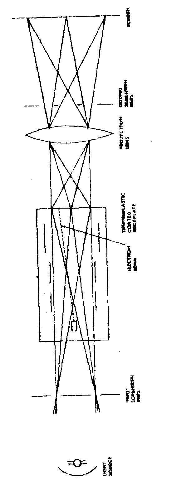
des.
Thus, the luimatron certainly has potential for use in real
time incoherent-to-coherant holographic image conversion
systems which need such a device for their successful implementation
/3/.
ElASTOMER
DEVICES
If the
thermoplastic material in thermoplastic deformation devices
discusses in the preceding section is replaced by an elastomer,
another useful device for holographic imaging (but not permanent
storage) is created. Such a device, the "ruticon"*,
has been investigated toy Sheridon /56/.
The
ruticon device has a layered structure consisting of a conductive
transparent substrate, a thin photoconductor, a thin defonnable
elastomer layer, and a defortnable electrode.The deformable
electrode can take three format (1) a conductive liquid,
(2) a conductive gas, or (3) a thin optically opaque flexible
metal; the separate devices resulting from these three different
deformable electrodes are identified, respectively, as a
ruticon, ruticon, and ruticon.The most interesting of these
is the ruticon. In operation, a deelectric field (< 600
V) between the thin flexible metallic electrode and the
transparent electrode establishes the initial uniform charge.
Holographic information impinging on the device through
the transparent substrate causes changes in the electric
fields across the photoconductor and hence across the elastomer.
These fields create mechanical forces which cause the elastomer,
and consequently the thin natal layer, to deform and form
a phase hologram.
In readout,
light is reflected with high efficiency from the metal layer
to reconstruct the original object wavefront. If the metal
layer is non-transparent, readout light will not affect
the conductivity modulation of the photoconductor layer.
In some forms, the permanence of ruticon storage may be
en-
hanced
by utilizing an image locking mode. Erasure is accomplished
by removing the do field. This is a distinct advantage over
the lumatron where heating is required for erasure.
LIQUID
GYSTAL - PHOTOCONDUCTOR DEVICE
The
ability to store optical images in liquid crystals /57/
has promted their use 'in both electrically- and photoconductively-controllable
real-time imaging devices. Kieinie and Wolff /58/ have reported
recyclable holographic storage in an electrically-controllable
device consisting of mixed (90% Hematic, 10% cholesteric)
liquid-crystal sandwich cells having matrix-shaped electrodes.
Holographic recording was achieved as a result of dynamic
scattering induced by application of a do or low frequency
ac electric field across the electrodes. While initially
the nematic ordering is intact and the nematic-cholesteric
mixture is clear the dynamic scatlaring caused by the applied
field emulsifies the cholesteric material. Because this
colloidial-like suspension can influence the coherence of
an incident laser light wavefront, holographic recording
is feasible. Recent experiments /58/ indicate that this
optical scattering state can persist for weeks without a
sustaining field or can be erased by an ac field in 20-500
ms. A typical restoration field strength is 5 V. m-1
(rms) at 3 kHz.
The
matrix-shaped electrode structure required for the electrically-controllable
device is complicated to construct and, worse, limits resolution
capability. The implementation of the photoconductively-controlled
liquid crystal device overcomes, in pronciple, both of these
problems. Such a device is achieved simply by replacing
the electrode matrix structure by a photocon - ductive layer.
Of the photoconductive materials tested, zinc sulfide /59/
(ultraviolet recording) and cadmium sulfide /60/ (visible
light recording) have given the best results thus far. Holographic
recording has not yet been reported, however, because resolution
of the device is on the order of only a few line-pairs per
millimeter. In structure, the device consists of a layer
of liquid crystal and a layer of photoconductor sandwiched
bet-
ween
two electrode layers of conductive material (e.g., tin oxide).
The photoconductive layer is designed to have a "nonilluminated"
resistance that is lower. In the nonilluminated condition,
an applied dc voltage across the electrodes of the device
lies alciost entirely across the photoconductive layer.
Thus, the low voltage across the liquid crystal layer is
not sufficient to produce scattering effects and the liquid
crystal remains transparent. However, when a wavefront illuminates
the photoconductor, its resistance is lowered causing more
voltage to appear across the liquid crystal. This higher
voltage produces sufficient current to produce dynamic scattering
and allow image storage.
The
photoconductor-liquid crystal devices permit image recording
and readout at a rate controllable by the magnitude of the
applied voltage and composition of the material used. The
sensitivity appears to be better than that of other recyclable
materials, being several orders of magnitude greater than
that of photochromic films.
PHOTOCONDUCTOR-POCKEL'S
EFFECT DEVICES
Thie
device consists of a layer of photoconductive, electrooptic,
single crystal material covered by insulating dielectric
layers on one or both faces, and sandwiched between transparent
electrodes (or one electrode and a simple ohmic contact).
Experiments using highly resistive photoconductive ZnS and
Bi12SiO20 as the crystal materials
have been reported in the literature /61-63/. In operation,
a dc voltage applied across the material is modulated by
an incident optical wavefront in accordance with the photoconductive
properties of the crystal, thereby storing the information
in the wavefront structure. Since the material is simultaneously
electrooptic, readout of the stored electrostatic pattern
can be accomplished by the Pockel's effect; i.e., the pattern
is reconverted to an optical wavefront by local phase ratardations
resulting from the transmission of uniformly polarized light
through the material. The combination of both photoconductive
and electrooptic functions in a single material
has
an advantage over a device using separate laminated photo-conductive
and electro-optic films because of the fabrication problems
inherent in interfacing a multilayared structure of this
kind. On the other hand, the complexities involved fabricating
a uniform single material which optimally exhibits both
functions is actually more difficult than the interfacing
problem at the present state of the art.
The
ZnS and Bi12SiO20 materials used in
the reported devices are films on the order of 30-μm
and 150-μm thickness, respectively. At the present
state of the art, they appear to offer comparable resolution
capabilitys 10-μm and approximately 12 μm. images/Images
have been recorded and read out in both devices but tnere
have been no reported experiments of holographic storage.
SUMMARY
A comparison
of performance parameters for recyclable holographic storage
media is given in Table 1. In most cases we have listed
the "best" state-of-the-art material in the storage medium
column as an example although there may be potentially better
materials being investigated. Detailed information on these
may be found in the list of references accompanying this
paper.
Although
quantitative information for recyclable holographic storage
media is in a rapid state of flux, we have attempted to
offer a quantitative comparison in Table 1 by defining a
"Figure of Merit". In deciding on a reasonable definition
for this relative "tradeoff" value we have omitted record-
and erase-time parameters because they differ by such great
orders of of magnitude (e.g., picoseconds vs minutes). These
particular parameters can be considered independently in
any specific design application depending on the desirad
recycling speed. The remaining quantitative parameters (resolution,
readout efficiency, and write energy) listed in Table 1
thus yield the following definition:
Figure
of merit = 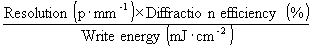
The
superior figure-of-merit values in Table 1 for the thermoplastic
and elastomer devices are due primarily to their low write
energy values. A look at the record time column, however,
indicates that their record time values are several orders
of magnitude higher than many media which have lower figure-of-merit
values. Also, the thermoplastic and elastomer devices require
more than light alone to operate properly, a fact which
dulls the meaning of their high figure of merit in certain
applications. In addition, the themoplastic device has poor
cycle lifetime at present and the elastomer device is not
useful for permanent storage.
Because
of their low write-enargy values, the liquid crystal-photoconductor
device and the photoconductor-Pockel'e effect device probably
have figure-of-merit values equivalent to those of the thermoplastic
and elastomer devices. However, since their diffraction
efficiency values are not available we cannot compute a
speciency figure of merit for them at present. Comparing
these devices further we note that the photoconductor-Pockel'e
effect device has exoellent sensitivity relative, to the
other recyclable media while the liquid crystal-photoconductor
device has poor resolution at present (although holographic
recording has been reported in the more complicated electrically-controlled
device /58/). On the other hand, the liquid crystal-photoconductor
device is simple in structure, has low power consumption,
and requires only low control voltages.
Generally
speaking, the thermoplastic, liquid crystal-photo-conductor,
and photoconductor-Pockel's effect devices can find significant
application as incoherent-to-coherent image converters /3/.
Most of the other materials in Table 1 find use in applications
in which frequent readout and infrequent write-in are required.
Reviewing
these other materials we see that magneto-optic materials
are quite useful for two-dimensional storage and have the
advantage of relative ease of fabrication compared to crystal
de-
vices
and the disadvantages of requiring accurate temperature
control and pulsad operation. Electro-optic materials are
useful for volume storage and therefore have high storage
capacity which, in turn, implies that selective erasure
is difficult. Also, being a single crystal material means
that are relatively expensive compared to film media. One
of their best advantages, however, is in nonoptically erasable
applications because holographic information can be "fixed"
in the material by a simple thermal process. In this respect,
electro-optic materials are superior to photochromic materials,
which, while three-dimensional storage materials in principle,
cannot be used as such because infonnation stored in them
cannot be fixed. Also, photochromic materials require two
wavelengths for operation but have inherently unlimited
resolution capability.
In the
photoconductor devices, although the photoconductive material
is not the key material for storagei it doss affect sensitivity
both in terms of amount of light required and the wavelength
which can be used, and it affeota readout efficiency since
light is absorbed if reading out with the same wave-length
as writing in. In this regard, the real beauty of the FEPG
devices is their ability to retain information on read-out
when light is absorbed) in comparison, information in the
photoconductor-Pockel's effect device decays on readout.
In summary,
Table 1 presents both quantitative and quntitative information
on the state of the art of recyclable holographic recording
media. The calculated figures of merit are intended only
as an indication of possible potential performances since
the state of the art in this area is so fluid at present
a very careful and perhaps partly intuitive tradeoff must
be made among all performance parameters for any projected
application.
|
Figure
of Merit
|
100
|
24
|
740
|
120
|
8
|
Readout
efficiency unknown
|
7*106
(theoretical)
|
1,5*105
|
Readout
efficiency unknown
|
Readout
efficiency unknown
|
|
Decay
Time (Dark Storage)
|
Indefined-limited
by humidity
|
Weeks
to months
|
Minutes
to months
|
Indefinite
|
Indefinite
|
Indefinite
|
Indefinite
|
Not
a permanent storage device
|
Unknown
|
~hours
|
|
Cycle
LifeTime
|
Read
|
∞
|
Reading
at same λ as writing destroys informa-tion
|
Blenching
occurs
|
∞
|
Indefinite
|
Indefinite
|
∞
|
Depends
on device structure
|
Unknown
|
Unknown
|
|
Write-Erase
|
Indefinite
|
Indefinite
|
Indefinite
|
~10
cycles
|
>105
cycles
|
Limited
by fatigue (see text)
|
100
cycles
|
>104
cycles
|
Unknown
|
Unknown
|
|
Readout
|
Resolution
(lp*mm-1)
|
~1000
|
~1500
|
~10000
|
~1000
|
~800
|
~50
|
~1000
|
~1000
|
~10
|
~1000
|
|
Line-arity
|
Fair
|
Good
|
Very
good
|
Good
|
Fair
|
Good
|
Good
|
Good
|
Good
|
Good
|
|
Readout
Efficiency (%)
|
10-2
(Faraday)
10-1
(Kerr)
|
80
|
1,2-3,7
|
6
|
10-2
|
Unknown
|
15
|
15
|
Unknown
|
Unknown
|
|
Type
of Hologram
|
Thin
phase
|
Thick
phase
|
Amplitude
|
Amplitude
|
Thin
phase
|
Thin
phase
|
Thin
phase
|
Thin
phase
|
Thin
phase
|
|
Recording
and Erasure
|
Erase
time
|
~μs
|
Same
as record
|
Same
as record
|
~1s
|
Same
as record
|
Same
or less than record
|
~1s
|
~10
ms
|
20-500
ms
|
~μs
|
|
Erase
Process
|
Same
as recording
|
Optically
or ther-mally in-duced charge redistribu-tion
|
Same
as recording
|
Redistribu-tion
by contained evapora-tion
|
Same
as recording
|
Heat
|
Removal
of electric field
|
Applica-tion
of ac electric field
|
Light
at appropria-te wave-length
|
|
Record
Time
|
10
ps - 50 ns
|
10
s -min
|
~ns
|
5-20
ns
|
~ms
|
~s
|
1
ms
|
~ms
|
<0,1
ms
|
~μs
|
|
Write
Energy (mJ*cm-2)
|
10
|
103-5*105
|
50
|
50
|
1
|
10
|
10-3
(theore-tical)
|
10-1
|
~5*10-3
|
~10-4
|
|
Recording
Process
|
Heating
above Curie point
|
Optically
induced charge separation
|
Optically
induced charge transfer
|
Evapora-tion
by heating
|
Light-modulated
ferro-electric switching
|
Electric
field pro-duced de-formation of heated material
|
Electric
field produced deforma-tion
|
Light-modulated
dynamic scattering
|
Light-modulated
electro-optic effect
|
|
Reference
|
5-13
|
14-19
|
20-29
|
30
|
38-43
|
34,
35
|
47-55
|
56
|
59,
60
|
61,
63
|
|
Material
or principal material material in device
|
MnBi
|
LiNbO3
|
Many
types (see text)
|
Bi
|
Bi4Ti3O12
|
PLZT
|
Staybelite
|
Siloxane
(τ - ruticon)
|
Mixed
liquid crystal: ZnS, CdS photo-conductor
|
Bi12SiO20
|
|
Storage
Medium
|
Magneto-Optic
Materials
|
Electro-Optic
Materials
|
Photo-Chromic
Materials
|
Metal
Films
|
Ferroelectric
Photo-conductor
Devices
|
Thermo-plastic
deformation Devices
|
Elastomer
devices
|
Liquid
Crystal-Photo-conductor Devices
|
Photo-Conductor
-Pockel's Effect Devices
|
REFERENCES
1. J.A.Rajchman.
Appl. Phys., vol.41, p.1376, 1970.
2. R.A.Bartolini,
W.J.Hannan, D.Karlsons, M.J.Lurie. Appl. Optics, vol.9,
p.2283, 1970.
3. N.H.Farhat,
W.R.Guard. Proc.IEEE, vol.58, p.1955, 1970.
4. J.J.Amodai.
CRC Handbook of Lasers with Selected Data on Optical Technology,
The Chemical Rubber Co., Cleveland, Ohio, 1971.
5. L.Mayor.
J.Appl.Physics, vol.29, p.1003, 1958.
6. L.Mayer.
J.Appl.Physics, vol.29, p.1454, 1958.
7. D.Chen,
J.P.Ready, E.Bernal. J.Appl.Physics, vol.39, p.3916, 1968.
8. R.S.Mezrich.
Appl.Phys.Letters, vol.40, p.132, 1969.
9. G.Y.Pan,
K.Pennington, J.H.Greiner. J.Appl.Physics, vol.40, p.974,
1969.
10.
M.J.Freiser. IBEB Trans.Magnetics, vol.MAG-4, p.152, 1958.
11.
R.S.Mezrich. Private Communication.
12.
N.Goldberg. IEEE Trans.Magnetics, vol.MAG-3, p.605, 1967.
13.
D.I.Iehemev, O.W.Lewicki. IEEE Trans.Magnetics, vol.MAG-4,
p.75, 1968.
14.
F.S.Chen, T.T.LaMacchia, D.B.Fraser. Appl.Phys.Letters,
vol.13, p.223, 1968.
15.
J.B.Thaxter. Appl.Phys.Letters, vol.15, p.210, 1969.
16.
J.J.Amodei, D.L.Staebler, A.W.Stephens. Appl.Phys.Letters,
vol.18, p.507, 1971.
17.
F.S.Chen. J.Appl.Physics, vol.40, p.3389, 1969.
18.
J.J.Amodei, W.Philllps, D.L.Staabler. IEEE J.Quan.Elac.,
vol.QE-7, p.321, 1971.
19.
J.J.Amodei, D.L.Staebler. Appl.Phys.Letters, vol.18, p.540,
1971.
20.
G.Jackson. Optica Acta, vol.16, p.1, 1969.
21.
S.Herman. Proc.Symp.Modern Optics, p.743. John Willey and
Sons, New York, 1967.
22.
J.P.Kirk. Appl.Optics, vol.5. P.1684, 1966.
23.
R.J.Araujo. Recent Advances in Display Media. NASA Symposi-
um Proceedings,
Cambridge, Mass., p.63, 1967.
24.
D.R.Bosomworth, H.J.Gerritsen. Appl.Optica, vol.7, p.95,
1968.
25.
A.S.Mackin. Appl.Optica, vol.9, p.1658, 1970.
26.
T.A.Shankoff. Appl.Optics, vol.8, p.2282, 1969.
27.
A.L.Mikaelian., A.P.Axenchikov, V.I.Bobrinev, E.H.Gulaniane,
V.V.Shatun. IEEE J.Quantum Elec., vol.EQ-4, p.757, 1968;
Soviet Physics-Doklady, vol.13, p.810, 1968.
28.
M.Lescinsky, M.Miller. Optics Communications, vol.1, p.417,
1970.
29.
D.L.Ross. Appl.Optics, vol.10, p.571, 1971.
30.
J.J.Amodei, R.S.Mezrich. Appl.Phys.Letters, vol.15. p.45,
1969.
31.
R.M.Schaffert. U.S.Patent 3, 146, 354, 1964.
32.
S.E.Cummuns. Proc.IEEE vol.55, p.1536, 1967.
33.
S.E.Cummuns, L.E.Cross. J.Appl.Physics, vol.39, p.2268,
1968.
34.
J.R.Maldonado, A.L.Meitzler. Proc.IEEE, vol.59, p.368, 1971.
35.
J.R.Maldonado, L.K.Anderson. IEEE Trans.Elec.Dev., vol.
ED-18, p.774, 1971.
36.
A.D.Morrison, F.A.Lewis, A.Miller. Ferroelectrics, vol.1,
p.75, 1970.
37.
M.M.Hopkins, A.Miller, Ferroelectrics, vol.1, p.37, 1970.
38.
S.A.Keneman. G.W.Taylor, A.Miller, W.H.Fonger. Appl.Phys.
Letters, vol.17, p.173, 1970.
39.
S.E.Cummins, T.E.Luke. IEEE Trans.Elec.Dev., vol.ED-18,
p.761, 1971.
40.
S.A.Keneman, G.W.Taylor, A.Miller. Ferroelectrics, vol.1,
p.227, 1970.
41.
S.A.Keneman, A.Miller, G.W.Taylor. Appl.Optics, vol.9, p.2279,
1970.
42.
G.W.Taylor, S.A.Keneman, A.Miller. Appl.Optics, vol.2, p.11,
1971.
43.
S.A.Kenenan, A.Miller, G.W.Taylor. Ferroelectrics, vol.3,
p.131, 1972.
44.
W.C.Stewart, L.S.Cosentino. Ferroelectrics, vol.1, p.149,
1970.
45.
W.J.Takel, N.P.Formigoni, M.H.Francombe. Appl.Phys.Letters,
vol.15, p.256, 1969.
46.
S.Y.Wu,W.J.Takei, M.H.Francombe, S.E.Cummins. Ferroelectrics,
vol.3, 1971.
47.
W.E.Glenn. J.Appl.Phys., vol.30, p.1870, 1959.
48.
W.E.Glenn. J.SMPTE, vol.74, p.663, 1965.
49.
J.C.Urbach, R.W.Meier. Appl.Optics, vol.5, p.666, 1966.
50.
L.H.Lin, H.L.Beauchamp. Appl.Optice, vol.9, p.2088, 1970.
51.
J.Urbach, R.W.Meier. Appl.Optics, vol.8, p.2269, 1969.
52.
H.R.Andereon, Jr., E.A.Bartkus, J.A.Reynolds. IBM J.Res.
Develop., p.140, 1971.
53.
L.S.Chang. Photographic Science and Engineering, vol.12,
p.238, 1968.
54.
R.J.Doyle, W.E.Glenn, IEEE Conf.Record 1970 IEEE Conf. on
Display Devices (70 C.55-ED), p.88, 1970.
55.
R.J.Doyle, W.E.Glenn. IEEE Trans.Electron Devices, vol.ED-18,
p.739, 1971.
56.
N.K.Sheridon. IEEE International Electron Devices Meeting,
Washington, D.C., 1970.
57.
G.H.Heilmeier, J.E.Goldmacher. Proc.IEEE, vol.57, p.34,1969.
58.
H.Kiemle, U.Wolff. 1970 Annual Meeting of Optical Society
of America, 1970.
59.
J.D.Margerum, J.Nimoy, S.Y.Wong. Appl.Phyc.Letters, vol.17,
p.51, 1970.
60.
G.Assouline, M.Hareng, E.Leiba. Proc.IEEE, vol.59, p.1355,
1971.
61.
D.S.Oliver, P.Vohl, R.E.Aldrich, M.E.Behrndt, W.R.Buchan,
R.C.Ellis, J.E.Genthe, J.R.Goff, S.L.Hou, G.McDaniel. Appl.Physics
Letters, vol.17, p.416, 1970.
62.
D.S.Oliver, W.R.Buchan. IEEE Trans.Elec.Dev., vol.ED-18,
1971.
63.
S.L.Hou, D.S.Oliver. Appl.Phys.Letters, vol.18, p.325, 1971.
|
|
|
|
|
 |
 |
 |
 |
|
Copyright
© 1999-2004 MeDia-security,
webmaster@media-security.ru
|
|
|


