1. SUBMIT TO: E105
2. SUBMIT EACH ABSTRACT TO ONE CONFERENCE ONLY.
Practical Holography XV
Stephen A. Benton
3. ABSTRACT TITLE: Use of materials on a basis As2S3 - As2Se3 for manufacture of holographic optical elements.
AUTOR LISTING:
Ivan I. Burdiyan, Karla Libknekhta str. No 176, flat 1, Tiraspol, 3300, Moldova
Igor S. Feshchenko, Benderskogo vosstanja str. No 3, flat 22, Benderi 278100, Moldova, feshchenko@mail.ru;
Yury N. Vigovsky, Novoslobodskaja str. No 31/1, Moscow, 103055, Russia, vigovsky@dol.ru
Valery S. Feshchenko, Benderskogo vosstanja str. No 3, flat 22, Benderi 278100, Moldova, feshchenko@mail.ru;
5. PRESENTATION: Poster Presentation
6. ABSTRACT TEXT:
The chalcogenide glasslike materials on a basis As2S3 - As2Se3 are widely applied in various fields of a science and technology. It is connected with their such properties, as wide spectral sensitivity, high resistance and high photoconduction, ability to photostructural transmutations and also with simplicity of their production.
We was studing the photographic and holographic properties of photoresist on a basis As2S3 - As2Se3 which was doped by metals. The including into a system of metals IV of group has allowed to increase holographic sensitivity of a photoresist and has expanded a spectral range of a material. Nonequilibrium doping of a photoresist by tungsten has made process of photostructural transmutations more controllable, what permit to obtain on the same material, both phase images with high contrast, and halftone images.
The dependence of photographic and holographic propertyes of investigated materials for various parameters of process and types of used etchants are demonstrated also.
7. KEY WORDS: Chalcogenide glasslike semiconductors, photoresist, photostructural transmutations.
8. BRIFF BIOGRAPHY:
Ivan I. Burdiyan finished in 1952 the Kishinev State University and A.F. Ioffe Physics-Technical Institute post-graduate course in 1969. In 1969 he has received the DSc degree in this Institute. In 1973 he has received the professor degree in Lvov State University. He works as the professor of the Dniestr State University, 25 October str. 128, Tiraspol, Moldavia and carry out researches on a semiconductors technology.
Use of materials on a basis As2S3-As2Se3 for manufacture of holographic optical elements.
Ivan I. Burdiyan1, Igor S. Feshchenko1, Yury N. Vigovsky2, Valery S. Feshchenko1
1Dniestr State University, 25 October str. 128, Tiraspol, Moldavia, feshchenko@mail.ru.
2MeDia Co, Novoslobodskaja str. No 31/1, Moscow, Russia, vigovsky@dol.ru.
Abstract
In this paper we was studing the photographic and holographic properties of photoresist on a basis As2S3 - As2Se3 which was doped by metals. The including into a system of metals IV of group has allowed to increase holographic sensitivity of a photoresist and has expanded a spectral range of a material. Nonequilibrium doping of a photoresist by tungsten has made process of photostructural transmutations more controllable, what permit to obtain on the same material, both phase images with high contrast, and halftone images.
1. Introduction
The chalcogenide glassy semiconductors (CGS) [1] already for a long time, call huge interest (more than 400 000 references in a Internet). They are widely employed for manufacturing of waveguides [2], of elements of integrated optics [2,7], of acoustooptical modulators [3], of superfast semiconducting switches [4,5], of meshes of memory [1,6], of holographic optical elements [1], of the holograms [1] and are used as photoresists for a nanolithography [1,8]. The virtues of CGS is the high velocity of switching, the high resolving power the wide spectral sensitivity range, the relative simplicity of deriving and the low cost.
But despite of a great many of articles on this theme until now up to an extremity the mechanisms of photostructural transformations happening in a CGS are not clear that does not allow to develop new gears and recording mediums.
Therefore the making of new semiconducting materials on the basis of CGS and study of mechanisms of photostructural transformations constitute topical task.
In work [1] was shown that an alloying of
chalcogenide glassy semiconductors by tin reduces to magnification
of photosensitivity at the expense of a normalization of a
matrix of a glass. In work [1] was shown the important influence
of metals of incidental subgroup of sixth group of periodic
table on increase of photosensitivity in a CGS. In this connection
we carried out experiments for showing up of influence of
these metals at a combined alloying on holographic properties
of a glassy semiconductor. For this purpose we used layers
of a CGS of composition (As2S3)0.3×
(As2Se3)0.7 which alloyed at a liquid melt by an dope of tin
0,015 at.% that according of our previous researches [9] raised
the photosensitivity in comparison with a nonalloyed semiconductor.
Also we investigated thin-film glassy semiconductors of composition
As2S3-As2Se3, As2S3-As2Se3:Sn 0.015 at. % and As2Se3 which
we nonequilibrium alloyed by a tungsten.
2. Experiments and discussion
We prepared the initial photosensitive mediums by a sequential
thermal spraying of layers WO2 and As2Se3-As2S3, As2S3-As2Se3:Sn
0.015at.%, in vacuum ~ 3×
10-3 Pa on glass substrates. For an oxide of a
tungsten of a thickness of layers amount 0,1-0,3 microns and
for As2Se3-As2S3 - 0,7-1 micron. If we used CGS of composition
As2Se3 the nonequilibrum alloying was carried out with the
help of thermal diffusion at room temperature. While CGS of
compositions As2S3-As2Se3 and As2S3-As2Se3:Sn 0.015at.% were
alloyed at temperature 80°
С during 5, 10, 15 and 20 minutes because at room temperature
the alloying was insignificant.
On these layers the diffraction gratings with spatial frequency
300 mm-1 were recorded.. We measured of diffraction
efficiency during an process of record of diffraction gratings.
The outcomes are presented on fig. 1. From the graph (fig.1.
a curve 1) it is visible the greatest sensitivity corresponds
to composition (As2S3)0.3×
(As2Se3)0.7 which was alloyed by tungsten by means of a thermal
diffusion at 80˚C within 5 minutes. Medium of same composition
(As2S3)0.3× (As2Se3)0.7 with
a underlayer WO2 but without a preliminary annealing has smaller
holographic sensitivity. A decrease of sensitivity for the
given medium is connected that the energy is expended not
only on photostructural transformations but also on a photodiffusion
of a tungsten in a layer of a CGS (fig.1. a curve 2). The
worst diffraction efficiency corresponded to structures containing
tin (fig.1. a curves 4-6). Apparently, the atoms of tin compete
with atoms of tungsten in the process of photostructural transformations.
Therefore diffraction efficiency was decreased.
For explanation of above outcomes we obtained absorption spectrums
of researched structures. A spectrum of an absorption of a
system As2S3-As2Se3:Sn 0.015at.% alloyed by tungsten differs
from the appropriate spectrum of a system As2S3-As2Se3 owing
to of small concentration of tin therefore we have considered
influence of a tungsten on an example of structure (As2S3)0.3×
(As2Se3)0.7. From fig.2. (a curves 1-5) we see what the spectrum
has appreciable change because of a thermal diffusion of ions
of a tungsten. There are two singularities on lengths of waves
606nm and 656nm if to carry out the annealing of sample during
5 minutes (fig.2. a curve 4). Further at magnification of
time of an annealing up to 10, 15 minutes of a singularity
disappeared (fig.2. a curve 3). And only at an annealing during
20 minutes appear two singularities but already on length
of waves 614nm and 670nm (fig.2. a curve 5). Such behavior
of a curve of absorption is connected in our opinion with
to origin of forming the ordered microareas of tungsten compounds
in CGS The dope of a tungsten are included in a CGS by two
ways: Its one part with concentration of an dope x1 is in
microareas, another - with concentration x2 is uniformly distributed
in a matrix of a glass, forming a homogeneous solid solution
(ideal glass).
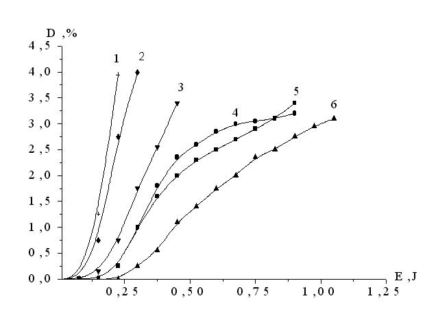
Fig.1. The graphs of an dependence of diffraction
efficiency from an energy of exposure:
1 - (As2S3)0.3× (As2Se3)0.7
with a underlayer WO2 an annealing 5 minutes.
2 - (As2S3)0.3× (As2Se3)0.7
with a underlayer WO2 without an annealing;
3- (As2S3)0.3× (As2Se3)0.7
with a underlayer WO2 an annealing 20 minutes;
4 - (As2S3)0.3× (As2Se3)0.7:Sn
0.015at.% with a underlayer WO2 an annealing 5 minutes;
5 - (As2S3)0.3× (As2Se3)0.7:
Sn 0.015at.% with a underlayer WO2 an annealing 20
minutes;
6- (As2S3)0.3× (As2Se3)0.7:
Sn 0.015at.% with a underlayer WO2 without an annealing.
The modifications in an absorption spectrum are connected with microareas which are responsible for extrinsic conduction in glassy chalcogenide semiconductors. They become apparent as singularities on lengths of waves 606, 614, 656 and 670nm (fig.2. a curve 4, 5). The displacement of an edge of a fundamental absorption in long wave area of spectrum is connected to formation of a series of solid solutions of a CGS with a tungsten. The tungsten dope which was in microareas and are identified by peaks 656nm and 670nm does not take part in photostructural transformations when carry out exposure of a system As2S3-As2S3 by He-Ne laser (l
=632,8nm) since after exposure these peaks do not disappear. The dope x1 which formed singularities on lengths of waves 606nm and 614nm take part in photostructural transformations at an exposure by light He-Ne of the laser. The dope x2 which has formed a homogeneous solution of a glass take part in photostructural transformations also. At an exposure of sample by integrated light both mode of tungsten dope take part in photostructural transformations. That become apparent because disappear singularities in an absorption spectrum and was moving an edge of a fundamental absorption into short-wave area of an absorption spectrum (fig.2. a curve 2.). I.e. the dope in microarea take part in photostructural transformations at the time of exposure by appropriate length of a wave. It permit to expand spectral sensitivity range of our materials into area of long wavelength of a spectrum.
The explanation of obtained spectra can
be the following at an annealing during five minutes at 80°
C of sample of structure As2S3-As2Se3 with a underlayer WO2
the singularity on length of a wave 606nm has place. It apparently
is connected to microareas the base of which make up the compound
of sulfur with a tungsten. The peak on length of a wave 656nm
is connected to microareas formed by compound of sulfur, selenium
and tungsten. At the further annealing during time 10 and
15 minutes of a singularity disappear but the edge of a fundamental
absorption was displaced into long wavelength area of spectrum
(fig.2. a curve 3). I.e. the homogeneous glass is formed.
The new microareas which absorb on lengths of waves 614nm
and 670nm are formed at an annealing within 20 minutes. They
are connected in our opinion with compound of a selenium and
tungsten, as these peaks earlier by us were observed at a
thermal diffusion of tungsten on layers As2Se3. At an exposure
by integrated light the full disappearing of singularities
occurs and the edge of a fundamental absorption is displaced
into short-wave area of a spectrum (fig.2. a curve 2).
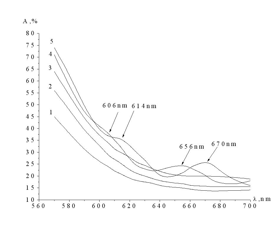
Fig.2. Absorption spectrums of layers of composition
As2S3 - As2Se3 with a underlayer WO2:
1 - not exposed layer;
2 - annealing of layers during 5 minutes
with a postexposure by integrated light
3 - annealing of layers during 10-15
minutes;
4 - annealing of layers during 5 minutes;
5 - annealing of layers during 20 minutes.
For clarification a nature of processes
happening in a CGS of alloyed by tungsten and for determination
of fitness of this practically of new material for manufacture
of the holographic optical elements we realized the etching
in various chemical etchants. In an outcome of these experiences
was found out that the solutions of alkali on base KOH,
NaOH dissolve faster exposed areas of films. But the etchants
on base of amine substances on the contrary dissolve faster
not exposed areas of films. Besides at magnification of
tungsten concentration in a system As2S3-As2Se3 the dissolution
of the exposed area of films in an amine etchant was considerably
worsened. And at tungsten concentration which correspond
to thickness d=0.3 micron of a underlayer WO2 the dissolution
practically was not observed. That has allowed to receive
diffraction gratings of 1000 mm-1 with diffraction
efficiency about 21 %.
Because of these experiments on etching
we suppose, that in an outcome of a thermal diffusion
of a tungsten in a system As2S3-As2Se3 there are compounds
of a type WS, WSe, WS2, WSSe, WSe2. Further during exposure
the tungsten compound which include the three atoms chalcogen
will formed i.e. compound of a type WSSe2.
3. Conclusions
In connection with above, it is possible to make
the following conclusions
1. The new material on base of CGS with increased holographic
sensitivity to light on length of a wave l
= 632,8nm is obtained.
2. Is shown, that the holographic sensitivity
on length of a wave 632,8nm has maximum for composition
As2S3-As2Se3. It is connected with that what the optical
breadth of a forbidden region coincides with an energy
of photons of a recording radiation. And also with existence
of microareas which is formed by compounds W-S.
3. The alloying by a tungsten has allowed
to expand a spectral range of a photosensitivity of structures
(As2S3)0.3× (As2Se3)0.7,
(As2S3)0.3× (As2Se3)0.7:Sn
0.015at.% and also has shown a possibility them of use
for recording of high contrasting and gray-scale picture.
Reference
- Electronic phenomena in chalcogenide glassy semiconductors.
Edited by K.D. Cendin, S-Petersburg: Nauka, 1996, 486p.
- Application chalcogenide glassy is semiconducting
in optoelectronics. Abstracts of the reports of the
second meeting - seminar, Kishinev, October 24-25, 1989,
83р.
- Handbook of laser with selected data on optical technology
/ Edited by R.J. Pressley / Chemical Rubber Co, Cleveland,
1971, 400 p.
- S.R. Ovshinsky Symmetric a gear of control by a current,
patent of USA № 3, 271.592б sq. pp. 307-885.
- S.Asokan, M.V.N.Prasad, G.Parthasarathy and E.S.R.
Gopal, Mechanical and Chemical Thresholds in IV-VI Chalcogenide
Glasses, Phys. Rev. Letts., 62, pp. 808-810. (1989)
- H.Frizsche, Switching and Memory in Amorphous Semiconductors:
J.Tauc (ed). Amorphous and Liquid Semiconductors. Plenum
Press, New York, 1974. pp. 313-359.
- H. Hisakuni and K. Tanaka Optical fabrication of microlenses
in chalcogenide glasses. Opt. Lett. v. 20, No. 9, pp.958-960.
(1995)
- B. Mednikarov Dependence of the dissolution characteristics
of As2S3 as a photoresist on the condensation rate and
evaporation temperature. J. Vac. Sci. Technol. B 7 (3),
pp. 561-564. (1989)
- I. Burdian, I. Feshchenko, Research of holographic
diffraction gratings made on a CGS of composition (As2S3)0,3×
(As2Se3)0,7, Proceedings BSFP-99, by ed. ac. Y.N. Denisuk,
Publishing house IGU: Irkutsk, 1999.- pp. 378-383.


